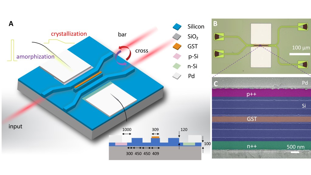
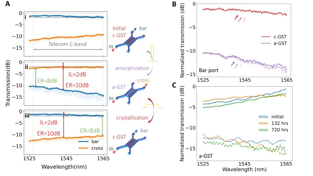
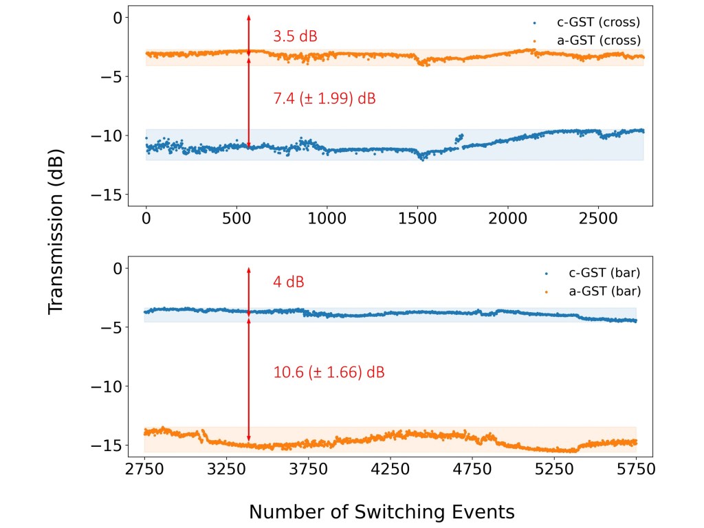
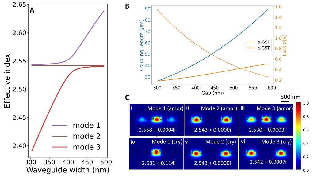
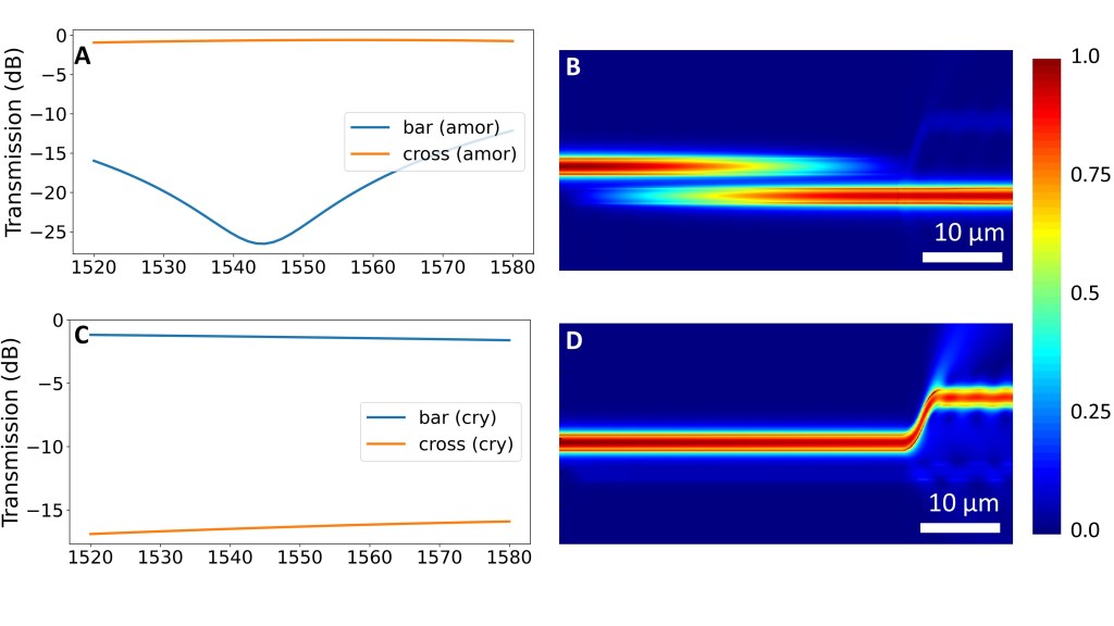
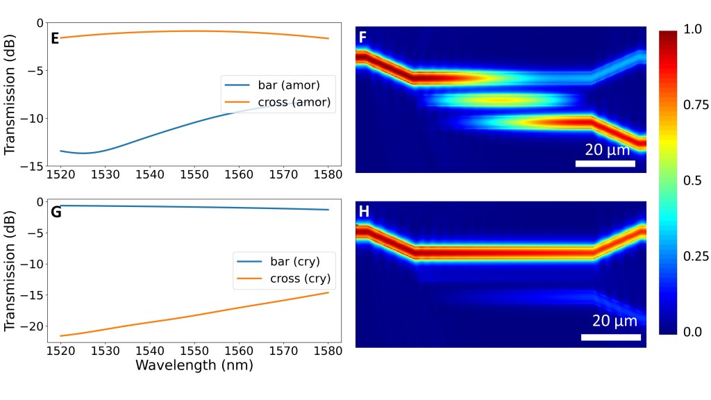
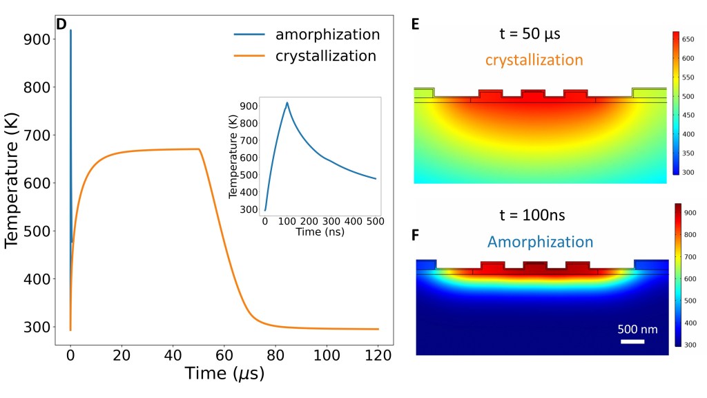
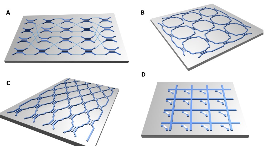
Figure 1. Broadband non-volatile electrically controlled 2 × 2 programmable unit in silicon photonics. (a) Device schematic. Inset: the cross-sectional view at the center of the device. The 40nm encapsulation Al2O3 is not shown. (b) The optical micrograph and (c) SEM images of the device. In the SEM image, the GST thin film, p++, and n++ regions are indicated by false colors.Figure 2. Characterizations of the electrically controlled 2 × 2 programmable unit. (a) Transmission spectrum of the device (i) initially, (ii) after applying an amorphization pulse (iii) after applying a crystallization pulse. The shaded areas are the measured raw spectra, and the solid lines are spectra after a low pass filter. IL and ER are insertion loss and extinction ratio, respectively. (b) Transmission spectra measured over three cycles at bar port. Each cycle is indicated with different color saturations. (c) Device functionality over an extended period of one month with a-GST. The solid and dashed lines correspond to the bar and cross port transmission.Figure. 3 Cyclability test of the electrically controlled 2 × 2 programmable unit. (Top) Transmission measured at the cross port. (Bottom) Transmission measured at the bar port. The blue/orange dots represent the measured transmission at 1550 nm after sending in a crystallization/amorphization pulse (with the same pulse condition in Fig. 2). The shaded regions correspond to variations of the two distinct transmission levels. A larger insertion loss of 3 dB at both ports at the beginning can be attributed to fiber alignment variation as well as the material degradation and thermal reflowing of the GST thin film in previous measurement steps, see Discussion Section.Figure S5. Mode simulation results for the 2 × 2 programmable units. (a) supermode effective indices changing with the HW width. (b) coupling length and loss with a/c-GST changing with the gap. (c) Mode simulation results. (i)(ii)(iii) First, second, and third-order modes when GST is in the amorphous state, (iv)(v)(vi) First, second, and third-order modes when GST is in the crystalline state.Figure S9. Transientheat transfer simulation results. (a)(d) The time-dependent temperature of the GST. The blue and orange lines are amorphization and crystallization pulses, respectively. The insets show zoom-in figures of the amorphization pulse. (b)(e) Temperature distribution at 50 µs for crystallization. (c)(f) Temperature distribution at 100 ns for amorphization. (a-c) 1 × 2 unit. (d-f) 2 × 2 unit.Figure S18. PIC schematics for various applications. (a) on-chip optical switching fabric. (b) multipurpose programmable PICs. (c) On-chip optical forward neural networks. (d) convolutional neural networks.