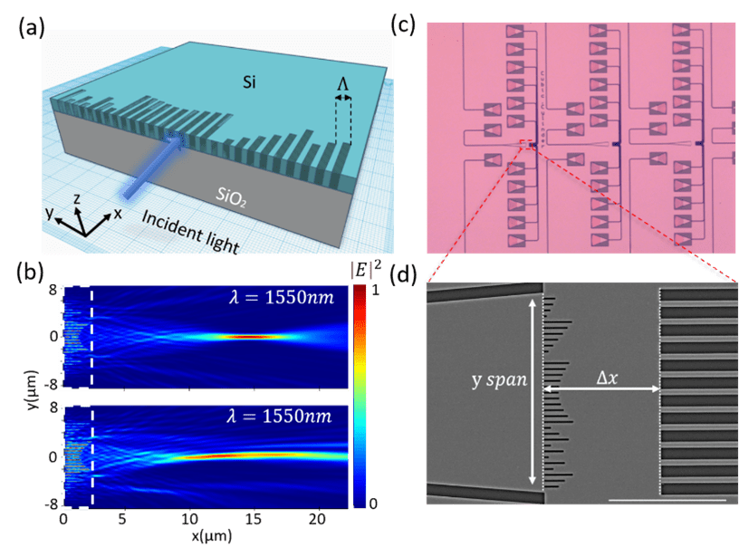
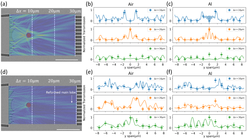
Figure 1. Design of on-chip synthetic-phase meta-optics. (a) Schematic showing the structure of 1D synthetic-phase meta-optics. The blue arrow indicates the direction in which the light is launched into the metalens. (b) Simulated electric field intensity of light focused by a quadratic meta-optics (top) and synthetic-phase meta-optics (bottom). The focal length is 15µm for both metasurfaces and of the synthetic-phase meta-optics is 0.025. The white dashed boxes highlight where the phase masks are. (c)Optica micrograph showing three synthetic-phase meta-optics of increasing . Grating couplers that are used to extract the light intensity at each port are also visible. (d) SEM image of a synthetic-phase meta-optics on SOI (scale bar:10µm).Figure 3. Self-healing of on-chip 1D accelerating beam. (a) SEM showing the quadratic metalens and the circular air pocket (scale bar: 10µm). The scatterer is highlighted with false color and the simulated electric field distribution is overlapped onto the SEM image. The white dashed lines indicate where the optical transmission is measured. (b) Intensity distribution across the y span showing the scattering of Gaussian beam by a circular air hole. (c) Intensity distribution across the y span showing the scattering of Gaussian beam by a circular Al scatterer. (d) SEM showing the synthetic-phase meta-optic and the circular air pocket (scale bar: 10µm). The reformed Airy-like main lobe is indicated by an arrow. (e) Intensity distribution across the y span showing the scattering of Airy-like beam by a circular air pocket. (f) Intensity distribution across the y span showing the scattering of Airy-like beam by a circular Al scatterer. Solid lines are the simulation results and dots are the measured data in experiment at each waveguide. Error bars in x are determined by the lateral span of the intensity point which equals to the 500nm waveguide width. Error bars in y are calculated from the standard deviation of grating coupler efficiency across the whole chip.